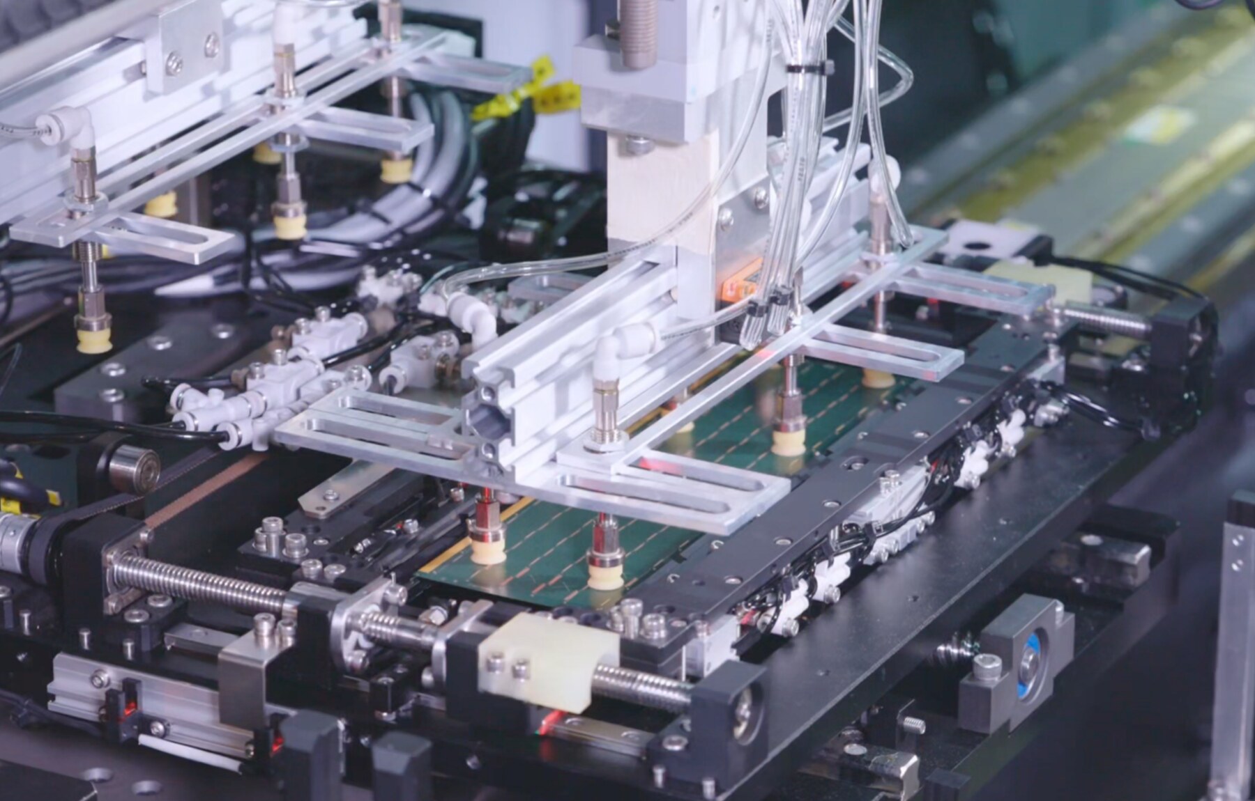
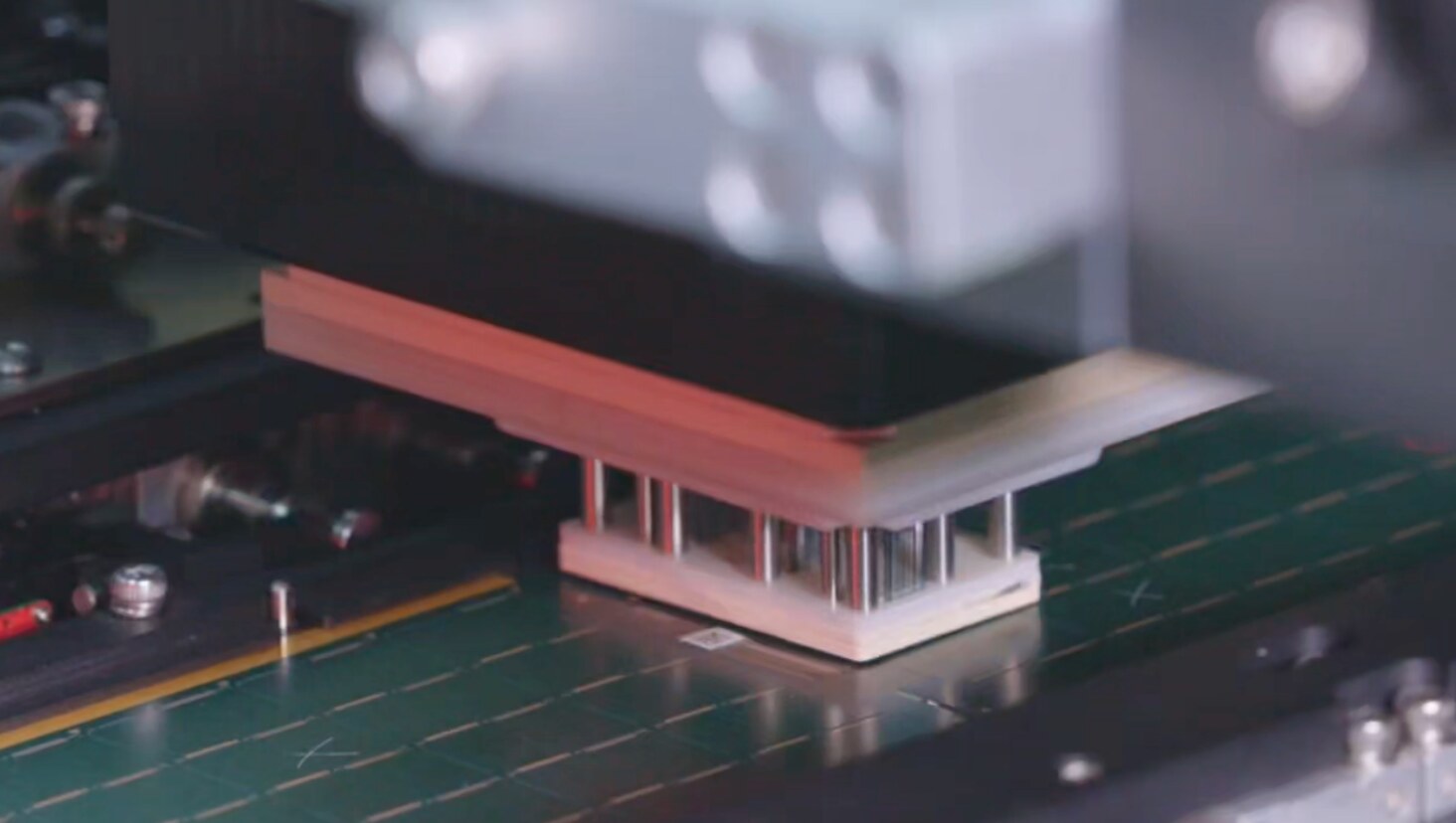
Singapore · Automated test systems

Silicon photonics test, engineered for production.

Automated optical, electrical and vision test platforms for wafers, laser dies, PICs, MEMS ICs and advanced substrates.

Wafer · Die · PIC
Test coverage
Optical · Electrical · Vision
Integrated measurements
R&D → Production
Scalable architecture
Axis-Tec silicon photonics test equipment
Core platform Automatic Silicon Photonics Wafer Level Tester
Test sequence
  1. 01 Locate
  2. 02 Align
  3. 03 Measure
  4. 04 Map

Product portfolio

Six platforms.
One test architecture.

Configure the motion, probing, optics, instrumentation and software around your device—not the other way around.

02Vision

Optical Facet Inspection

Automated imaging and defect review for optical facets, supporting consistent inspection before downstream assembly and test.

  • Multi-view imaging
  • Defect classification
  • Traceable review
View inspection details
03Laser

Laser Die Optical Test

Configurable optical and electrical characterization for laser dies, with automated handling, alignment and result binning.

  • Optical power
  • Spectrum
  • LIV
View laser tester details
04PIC

PIC Test

Flexible electro-optical test for photonic integrated circuits, from passive structures to active transmit and receive devices.

  • OO / OE / EO
  • DC / RF probing
  • Polarization control
View PIC tester details
05MEMS

MEMS IC Test

TPH environmental sensor, IMU and ambient-light IC test solutions spanning laboratory calibration through automated production.

  • TPH
  • IMU
  • ALS
View MEMS division
06Advanced IC

AI Chip IC Substrate Tester

Automatic electrical integrity test for HDI and IC substrates, with precision alignment, high-density switching and production handling.

  • Open / short
  • 4-wire
  • Leak / spark
  • CAD netlist
View substrate tester

actif. AS Series

Wafer-scale precision, configured for your test flow.

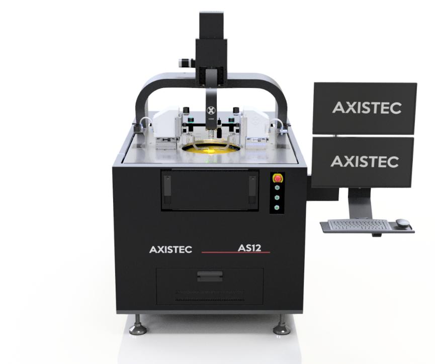
A fully integrated opto-electrical platform for automatic silicon photonics wafer and chip testing. The AS Series supports R&D characterization, engineering validation and high-volume production within one modular architecture.
Configure an AS system Standalone or loader-integrated
Axis-Tec AS12 automatic silicon photonics wafer level tester
AS128 / 12-inch wafer platform

Optical-access configurations

Three wafer-test paths, one modular platform.

The optical interface, wafer handling and measurement stack are configured around the device architecture and production flow.

01

Grating Coupler Wafer Level Test

Vertical optical access for surface grating couplers, with vision-guided positioning, fibre-array support, active alignment and wafer-level mapping.

02

Edge Coupling Wafer Level Test

Precision edge access for polished or prepared facets, using six-axis active alignment with single-fibre or fibre-array interfaces.

03

Glass-Wafer Photonics Test

Configurable optical and electrical test for glass-based photonic and interposer structures, with handling adapted to the substrate and test plan.

01 / Grating-coupler configuration

Approach the optical interface from above.

Vision-guided positioning brings the fibre interface to each surface grating. The six-axis alignment module then optimizes optical power before the configured measurements and wafer-map sequence run.
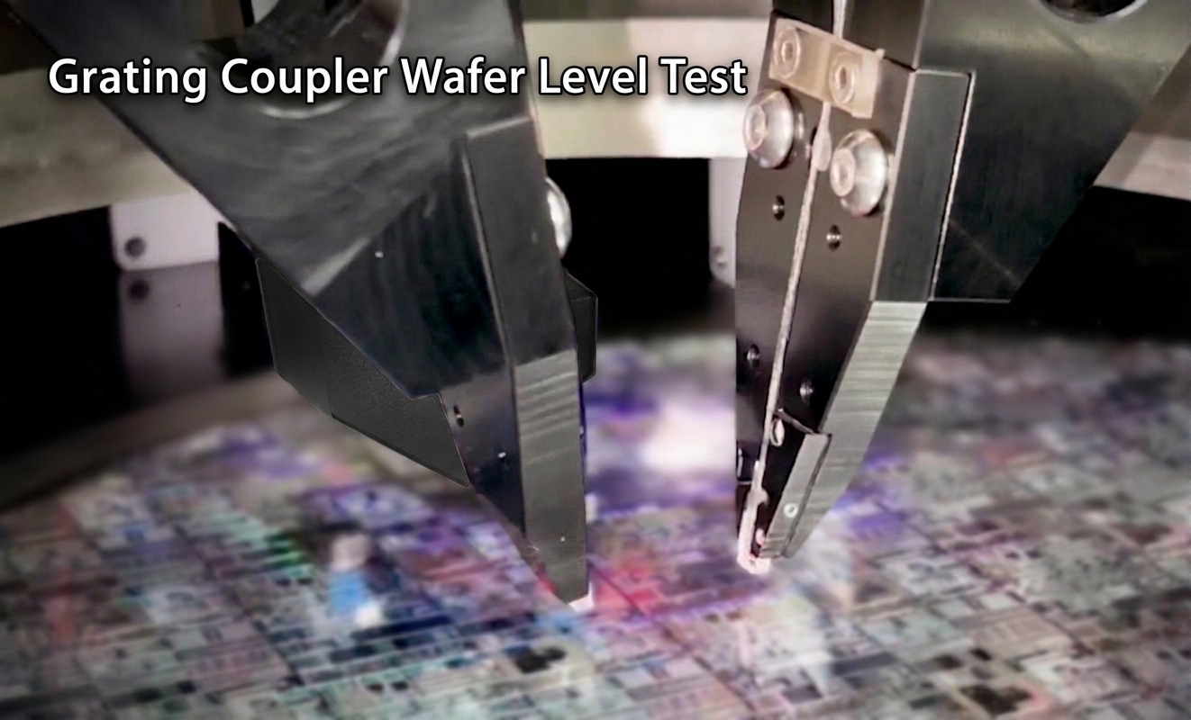
  • Vertical single-fibre or fibre-array access
  • Coarse and fine active optical alignment
  • Automatic stepping across the wafer map
Optical probes positioned above a silicon photonics wafer for grating-coupler wafer-level testing
Grating couplerVertical optical access at wafer level

02 / Edge-coupling configuration

Reach the prepared edge, then optimize coupling.

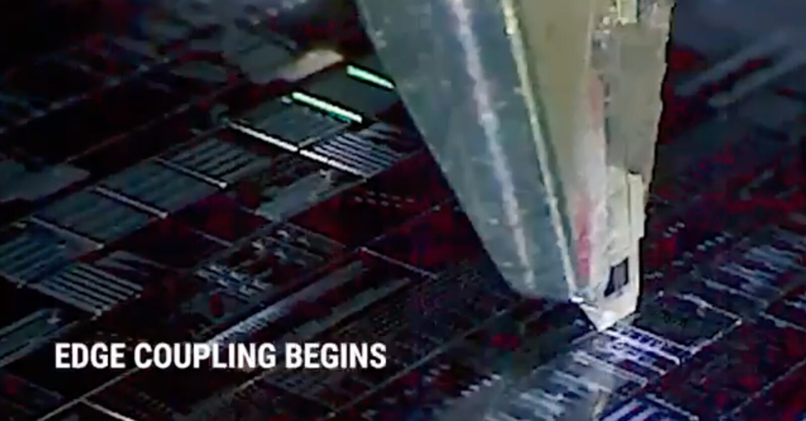
Edge access is configured around the wafer, die or interposer geometry. Vision brings the optical interface close to the coupling region before the six-axis module performs the final active power search.
  • Prepared or polished facet access
  • Single-fibre or fibre-array interface
  • Manual setup or recipe-driven alignment
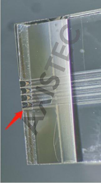
Close view of a prepared photonic edge with multiple optical coupling channels
Prepared edgeOptical channels at the facet
Optical probe approaching the edge of photonic devices for edge-coupling alignment
Alignment conceptControlled access to the coupling plane

03 / Glass-photonics configuration

Map, illuminate and collect through glass.

A configurable glass-wafer station combines XYR wafer positioning, height mapping, camera guidance and multi-axis optical alignment. The measurement path can be arranged for spot illumination, output collection and spectral analysis.


  • Wafer-height mapping and camera registration
  • Manual or automated six-axis coupling
  • Optical spectrum analysis integration
Glass photonics wafer test layout with XYR chuck, height sensor, camera, six-axis manipulators, fibre array and optical spectrum analyser
System conceptConfigurable glass-wafer optical test path
Representative applications of silicon photonics in co-packaged optics, AI optical interconnect and digital LiDAR
Representative applicationsCommunications · AI infrastructure · Digital sensing

Where it is used

From the wafer to high-bandwidth systems.

Telecommunications & CPO

Optical engines, transceiver building blocks and co-packaged optics for high-bandwidth data movement.

AI optical interconnect

Photonic I/O, optical chiplets and interposers designed to move data efficiently between accelerators.

Digital LiDAR

Emitter, receiver and photonic ranging devices for high-channel-count perception and industrial sensing.

Wafer8 / 12 inch350 × 350 mm XY travel
Alignment6-axis activeEdge and vertical grating
MeasurementsOO · OE · EO · EEOptical, DC and RF integration
ThermalUp to 200 °CBelow 0 °C available on request

01 / Precision motion

Wafer chuck & vision

Wafer chuck
8 / 12 inch
XY travel
Up to 350 × 350 mm
XY resolution
0.1 µm
XY repeatability
±1 µm
Programmable speed
Up to 70 mm/s
Microscope zoom
0.5× to 5×

02 / Optical alignment

PEAKQUEST 6-axis module

Active axes
X, Y, Z, θX, θY, θZ
XYZ travel
±20 mm
Linear resolution
0.05 / 0.02 / 0.01 µm
Rotational travel
±5°
Coupling
Edge / vertical grating
Fiber unit
Single fiber / fiber array

03 / Electrical probing

Programmable & mechanical probes

Programmable travel
±20 mm XYZ
Resolution
0.1 µm
Repeatability
±0.1 µm
Probe stations
Up to 2, north / south
Electrical test
Mixed signal, DC and HF
RF option
Up to 100G, north station

04 / Open test platform

Software & instrumentation

Test development
C# / NI TestStand
Customer integration
Python / LabVIEW / C++
Communications
GPIB / TCP-IP
Automation modes
Manual / semi / full
Wafer data
32-bit binning and map I/O
Instrument choice
Flexible brand integration

Opto-electrical coverage

One platform for passive and active PIC test.

OO

Insertion loss, spectral response, wavelength sweep and polarization-dependent loss.

OE

Illuminated DC I-V and S-parameter measurements, including bandwidth and return loss.

EO

S-parameters, wavelength and bias sweeps, insertion loss and optical power sweeps.

EE

DC I-V, C-V and L-V impedance sweeps for complete electrical characterization.
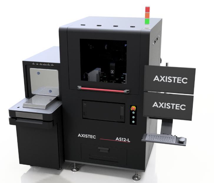
Axis-Tec AS12-L with integrated wafer loader and enclosure

Production automation

Loader-ready by design.

Run the AS Series as a standalone tester or extend it with wafer loading for inline production and reduced manual handling.

  • 8 / 12-inch wafer support
  • Single-cassette configuration
  • Automatic notch alignment
  • Wafer ID reader

Specifications are configurable by application. Contact Axis-Tec for the final system configuration and acceptance criteria.

Optical facet inspection

See the surface before it becomes a yield problem.

A configurable vision platform for inspecting fibre-array end faces and laser-die output facets. Defined inspection regions, consistent imaging and recorded pass/fail results help engineers review critical optical surfaces before assembly or optical test.
Configure an inspection system Inspection optics and acceptance criteria are configured to the device.
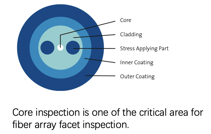
Diagram identifying core, cladding, stress applying parts and coating regions on an optical fibre end face
Fibre-array inspectionCore and surrounding regions
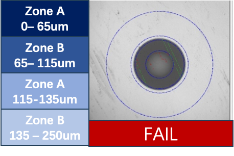
Example optical end-face inspection result with concentric inspection zones and a fail decision
Inspection resultZoned pass / fail review

01 / Fibre-array facets

Inspect the core—not only the connector.

The core is the most critical optical region. The inspection recipe can separate the core, cladding and coating into defined zones so each area is reviewed against the appropriate acceptance criteria.
  • Configurable concentric inspection zones
  • Consistent illumination, focus and image capture
  • Recorded image with pass/fail disposition
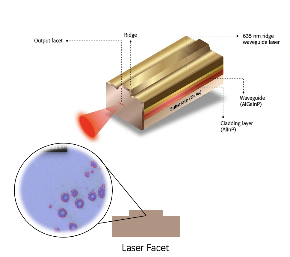
Laser ridge waveguide diagram and magnified laser output facet with highlighted surface defects
Laser-die inspectionOutput-facet defect review

02 / Laser output facets

Review the emitting surface at high magnification.

The system images the output facet around the ridge or emitting aperture and presents detected areas for review. This supports consistent inspection before die attachment, characterization or final assembly.

  1. 01LocateFind the facet or end face
  2. 02FocusSet repeatable imaging conditions
  3. 03InspectApply device-specific zones
  4. 04RecordSave image and disposition

Defect classes, zone dimensions and pass/fail limits are configured to the customer drawing and agreed inspection standard.

Laser die & COS characterisation

From electrical drive to optical performance—automatically.

An integrated platform for pick-and-place, thermal conditioning, active optical alignment and complete characterisation of chip-on-submount devices. Built around nominal 3 × 5 mm COS, with configurations spanning low-power evaluation to 50 W optical output.
Configure a laser die tester R&D characterisation · Engineering validation · Automated production
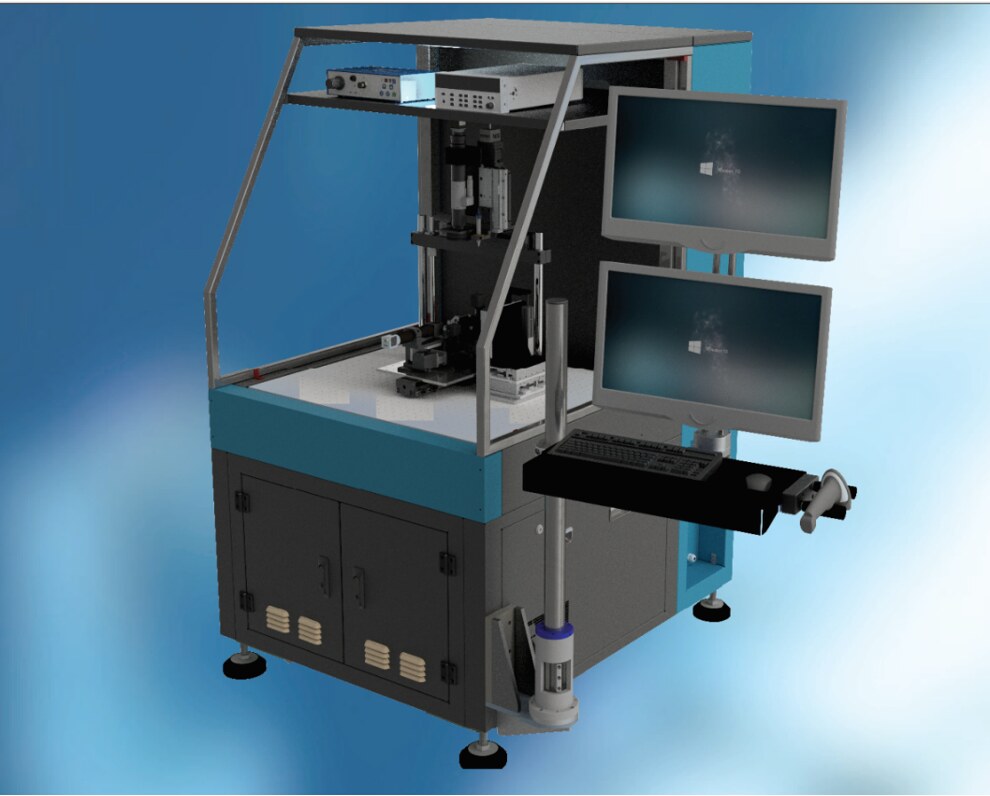
Laser die optical test station with automated motion, optics and dual monitors
Automated platformHandling · Alignment · Measurement
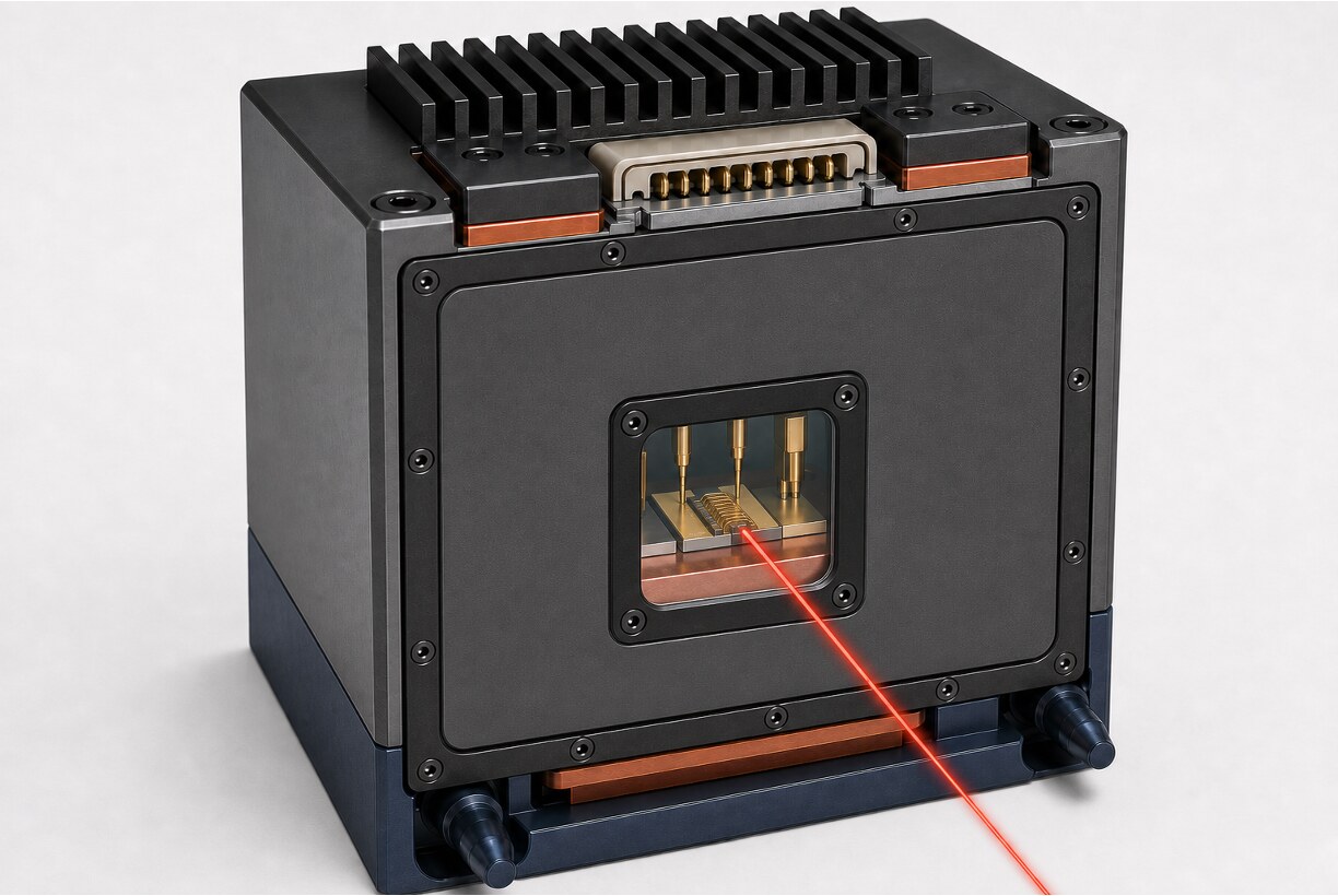
Enclosed laser die test fixture with electrical probes and optical path
Controlled test cellESD · CDA · Interlocks
Device3 × 5 mm COSNominal chip-on-submount format
Optical output50 mW–50 WConfiguration dependent
Electrical driveUp to 30 A / 2 V1.6 V nominal or application-specific
Wavelength800–1700 nmOptics and instruments configured by device
Temperature−10 to +45 °CControlled COS test condition
OutputsPIV · LIV · SpectrumPlus beam size and X/Y divergence

Automated measurement architecture

One recipe coordinates the device, optics and instruments.

The system aligns each COS to the required optical path and records electrical, power, spectral and beam-quality data at programmable operating-current points.
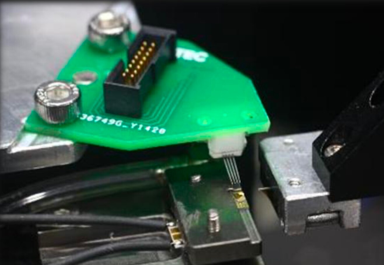
Chip-on-submount fixture with electrical contact and optical alignment hardware

01 / Device handling

Automatic COS pick, place and contact.

The handling module loads a nominal 3 × 5 mm chip-on-submount into an ESD-safe test fixture, establishes the electrical connection and positions the device for repeatable optical measurement.
  • Recipe-controlled pick-and-place sequence
  • Precision fixture location and electrical probing
  • Temperature conditioning at the device plane
  • Device identity and result traceability
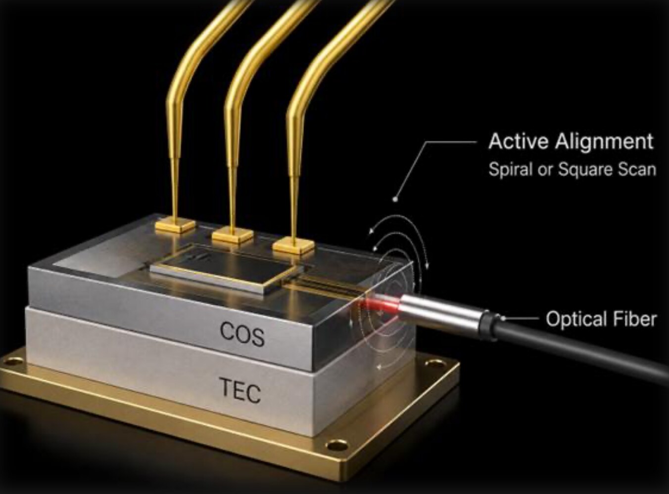
Diagram of active optical-fiber alignment to a laser chip-on-submount on a temperature-controlled stage

02 / Active alignment

Route the emission to the measurement that matters.

Programmable motion aligns the COS to an integrating sphere for total optical power, to the sphere’s fibre output and OSA for spectrum, or to a beam profiler for spatial beam analysis.
  • Coarse search followed by fine power optimisation
  • Integrating sphere and power-meter alignment
  • Fibre patch cord from sphere to optical spectrum analyser
  • Beam-profiler alignment for X/Y beam quality
  1. 01LoadPick and place COS
  2. 02ContactESD-safe electrical interface
  3. 03ConditionSet device temperature
  4. 04AlignSphere, OSA or profiler
  5. 05SweepProgrammable current points
  6. 06ReportCurves, spectra and beam data
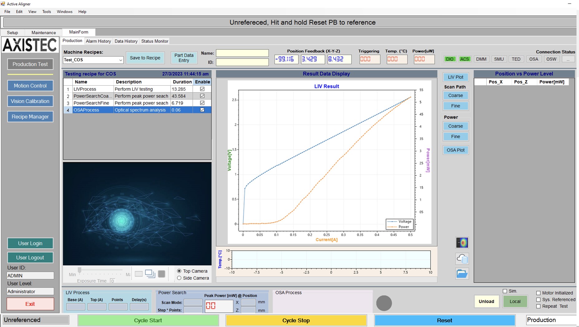
Axis-Tec Active Aligner software displaying a completed LIV result with voltage and optical-power curves
Actual LIV resultVoltage and optical power versus current

Characterisation & results

Every current point becomes a complete optical record.

At each programmed operating current, the controller coordinates the source, thermal stage and selected instruments. Power and spectrum can be synchronised at the same current set point through the integrating-sphere measurement path.

LIV / PIV

Optical power, drive current and forward voltage curves, including configurable limits and result binning.

Spectrum

Spectral capture across 800–1700 nm, with the optical path and analyser selected for the device wavelength.

Beam

Beam size and divergence on both X and Y axes at selected operating-current conditions.

Report

Automatic report package with plots, test conditions, instrument data, pass/fail status and exportable results.

Protected test environment

Designed for sensitive, high-power emitters.

ESD protectionGrounded handling, fixture and chamber provisions protect the COS through load, contact and test.
Humidity & condensation controlRH monitoring, CDA purge and dew-point control protect the device during sub-ambient operation.
System safetyThe final configuration can include access interlocks, current limits and laser-safety provisions appropriate to the application.

Performance ranges and measurement instruments are configured to the COS, fixture, optical path and agreed acceptance criteria.

Photonic integrated circuit test

Manual flexibility.
Automated repeatability.

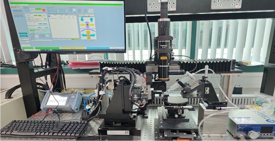
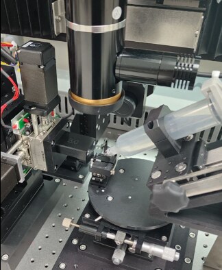
A configurable electro-optical platform for PIC characterization, engineering validation and production development. Operate it manually for process setup or automate device location, active alignment, measurement and result capture through a recipe.
Configure a PIC test system Optical and electrical instruments are selected for the device and test plan.
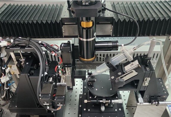
Axis-Tec photonic integrated circuit test station with motion control, microscope and optical instrumentation
Engineering platformManual or automatic PIC test operation
OperationManual · AutomaticDevelopment through repeatable recipes
AlignmentPEAKQUEST 6-axisClosed-loop optical power optimization
VisionPreset device locationAutomatic move to the alignment region
Test modesO–O · O–E · E–OPassive and active PIC coverage
Close view of optical manipulators aligned to a photonic integrated circuit under the microscope

01 / PEAKQUEST active alignment

Find and hold the optical peak.

The Axis-Tec six-axis manipulator positions the fibre or fibre array in X, Y, Z and angular axes. PEAKQUEST executes the selected coarse and fine search strategy to optimize coupling at the device.
  • Manual jog control for setup and recipe development
  • Automated multi-axis power search
  • Single-fibre or application-specific optical interface
Axis-Tec PIC test area showing PEAKQUEST manipulators, microscope and device fixture

02 / Vision-guided automation

Move close before active alignment begins.

The optional automatic vision system locates device features or returns to a stored alignment position. The motion system then transfers control to PEAKQUEST for the final optical search and recipe-controlled measurement sequence.

  • Device and feature location under the microscope
  • Programmed move to pre-set alignment coordinates
  • Automatic test execution and result traceability

Integrated test coverage

One station, three electro-optical signal paths.

O–O
Optical in · Optical out

Characterize passive optical paths, splitting, insertion loss and wavelength-dependent response.

O–E
Optical in · Electrical out

Stimulate photodetector and receiver structures optically while capturing the electrical response.

E–O
Electrical in · Optical out

Drive active transmitter, modulator or source structures and measure the resulting optical output.

Wavelength range, electrical bandwidth, probes, fibres and measurement instruments are configured to the PIC and acceptance criteria.

MEMS IC Tester Division

Three sensor domains.
One production path.

Axis-Tec combines controlled stimulus, multi-site contact, precision motion and automated handling for MEMS sensor calibration and functional test.
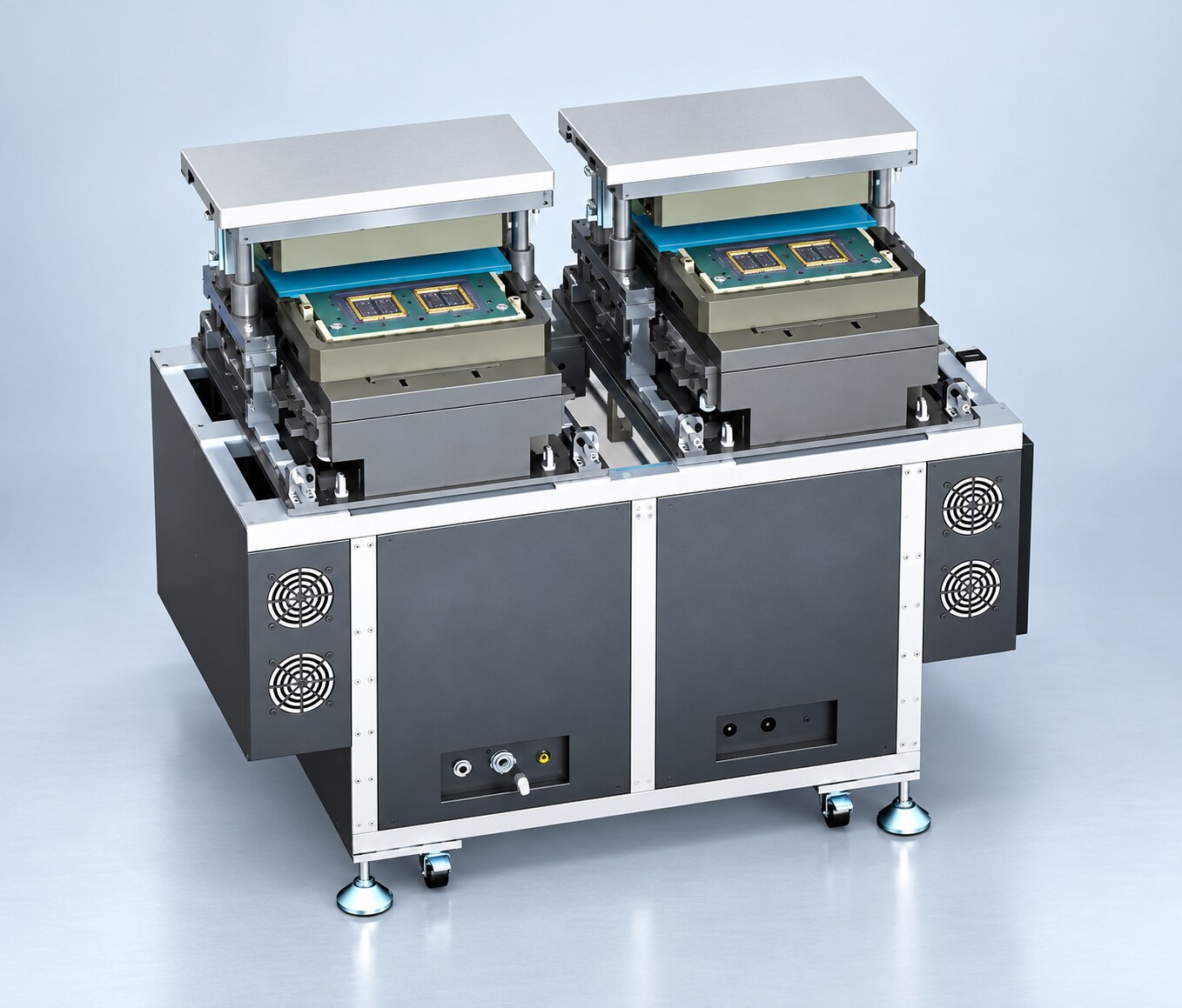
Professional render of the Axis-Tec dual-chamber TPH MEMS sensor stimulus unit

01 / Environmental sensors

TPH MEMS Sensor Testing

Laboratory and production systems for temperature, pressure and humidity sensor calibration, programmable stimulus and functional test.
Stimulus
Temperature · Pressure · Humidity
Temperature
−40 to +125 °C
Extended range
−55 to +150 °C
Production scale
Up to 256 sites
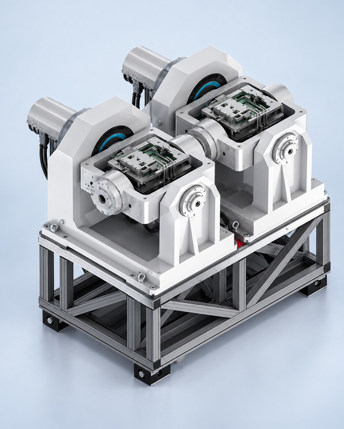
Professional render of the Axis-Tec dual-table MEMS IMU final-test system

02 / Inertial sensors

MEMS IMU Tester

High-precision calibration and test for accelerometers and gyroscopes, available as laboratory turntables or automation-ready final-test equipment.
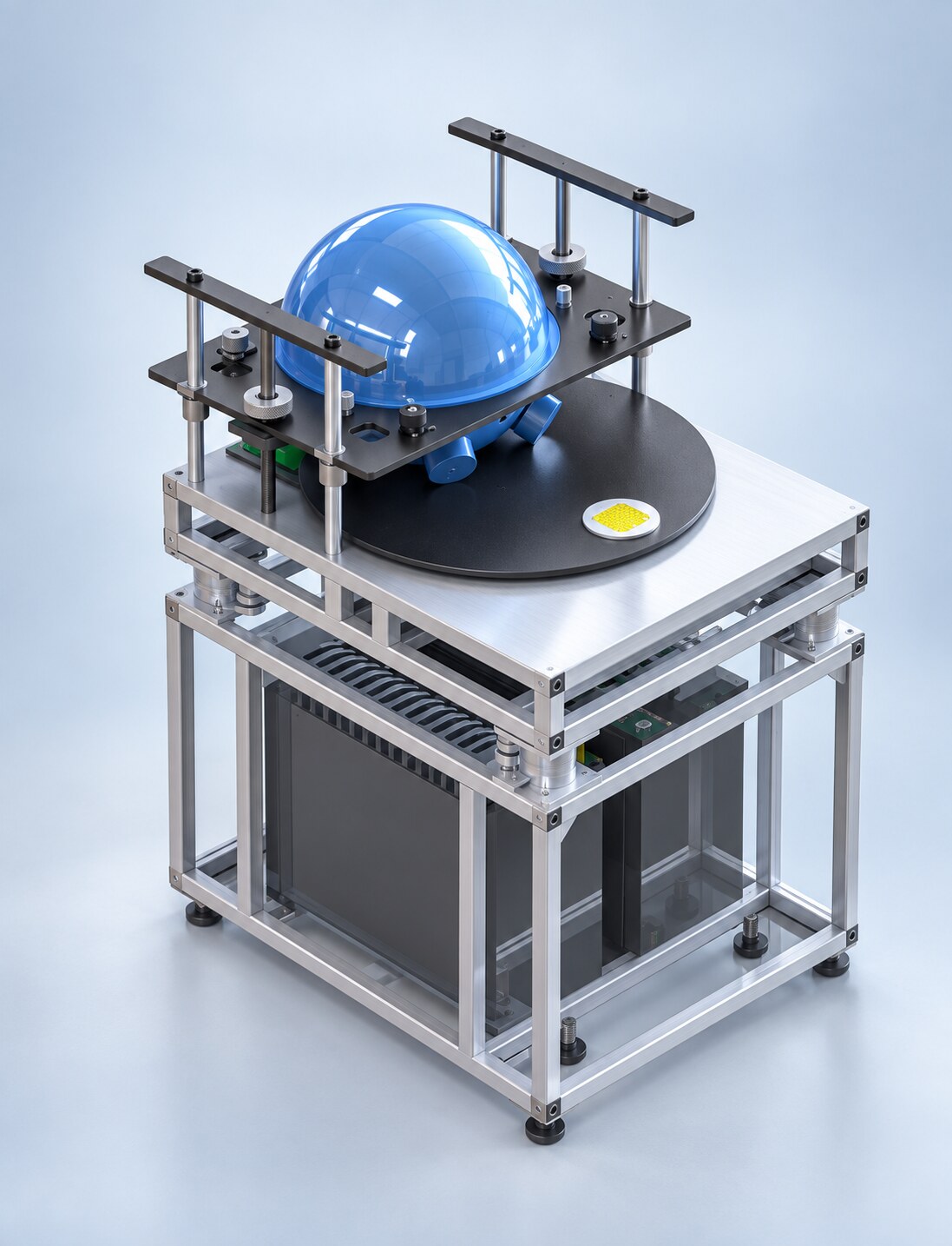
Devices
Accelerometer · Gyroscope
Architecture
Dual rotary tables
Parallel sites
64 × 2
Rate range
10–500 dps
Professional render of the Axis-Tec MEMS ambient light sensor test unit

03 / Optical sensors

MEMS ALS IC Tester

Programmable multi-colour illumination for ambient-light and optical sensor calibration, with continuous wavelength and colour-temperature monitoring.
Light channels
7 independent channels
Illuminance
0–3000 lux
Uniformity
≥98% at socket plane
Monitoring
Spectrometer feedback
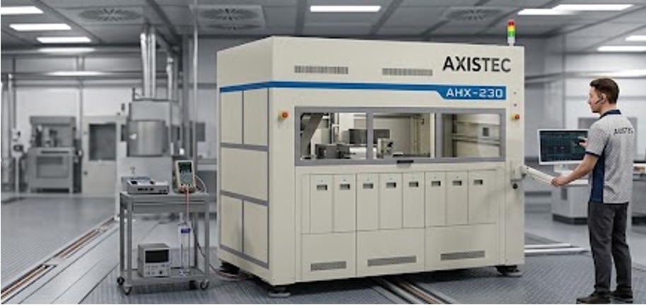
Axis-Tec AHX-230 enclosed automatic MEMS IC tester on a production floor
Production enclosureConfigurable for TPH, IMU or ALS IC test

Automatic test & sorting platform

One enclosure, configured around the sensor.

The enclosed MEMS IC tester can be fitted with the required TPH, IMU or ALS stimulus and measurement modules. After the programmed test and calibration sequence, the handler sorts each device into its assigned result bin.
  • Automatic device loading and contact
  • Sensor-specific stimulus and electrical test
  • Post-test pass/fail bin sorting
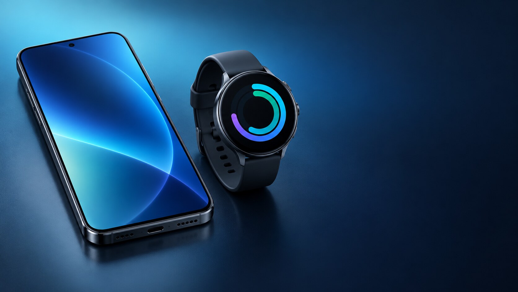
Generic smartphone and smartwatch representing applications for MEMS sensors
End productsSmartphones · Smartwatches · Wearables

Representative applications

Sensors inside everyday mobile devices.

Axis-Tec test platforms help sensor manufacturers calibrate and verify the compact devices that enable environmental awareness, adaptive displays and motion intelligence.

TPH
Environmental context

Barometric altitude, indoor navigation and temperature–pressure–humidity monitoring in selected handsets and wearables.

ALS
Adaptive light response

Automatic display brightness, daylight awareness and power-efficient screen control.

IMU
Motion intelligence

Screen rotation, gesture and activity tracking, navigation, fall detection and camera stabilization.

Sensor mix varies by device. IMU and ambient-light sensing are widely used; full TPH sensing is selected according to the product design.

Shared production architecture

From stimulus to sorted device.

  • Multi-site testScalable sockets and parallel test channels
  • Flexible handlingTray, wafer ring, tape-and-reel, bowl and tube
  • Factory integrationAutomated calibration, analysis, reporting and optional AOI
Discuss a MEMS application Final specifications are configured to the device, stimulus and throughput requirement.

AI chip & advanced packaging

Electrical integrity beneath the chip.

An automatic platform for HDI and IC substrates used in BGA, CSP and advanced-package applications. Precision vision alignment, dense electrical switching and automatic handling bring contact, measurement and traceability into one production system.
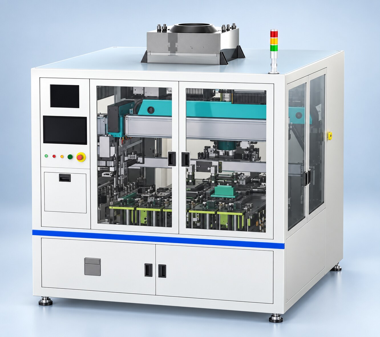
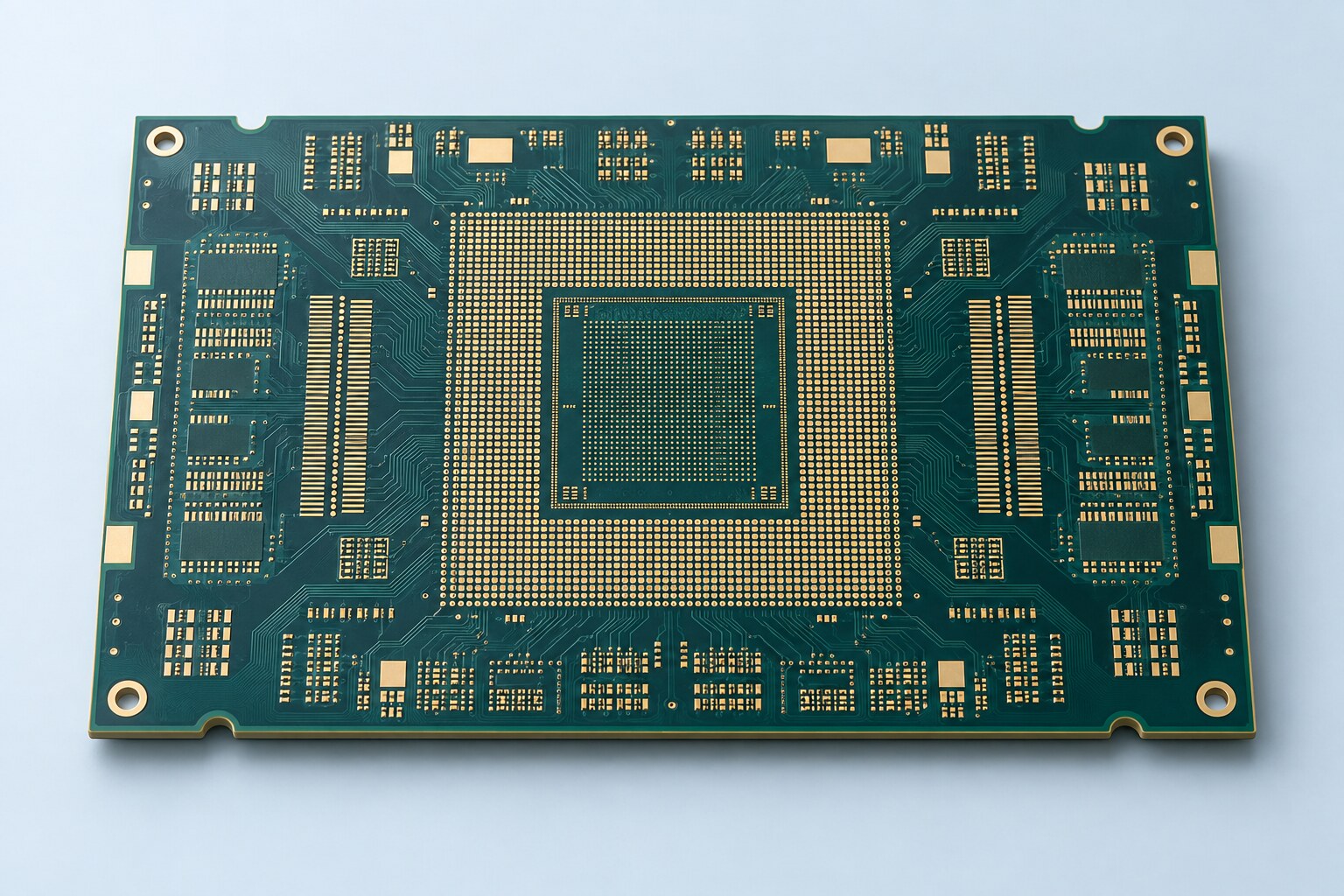
Discuss your substrate Configured to the substrate, fixture and factory flow
Professional render of the Axis-Tec automatic AI chip IC substrate tester
Automatic platformAI chip IC substrate tester
Illustrative high-density AI IC package substrate with fine-pitch contact arrays and routing
Example DUTHigh-density advanced IC substrate
Substrate size45 × 50 to 150 × 250 mmHDI, BGA, CSP and related formats
Test points8K standardOptional upgrade to 16K
Positioning±2.5 µmVision-guided automatic alignment
ArchitectureSingle test stationAutomatic contact and measurement
Axis-Tec IC substrate tester stage with automatic fixture positioning and contact hardware
Automatic test stagePosition · Contact · Measure
Close view of the IC substrate fixture head making contact with the substrate
Fixture interfaceRepeatable substrate contact

Fixture & CAD data compatibility

Move from the substrate design to a repeatable test layout.

FixtureStandard DD / QD

Supports standard DD and QD fixtures with a fixture height of 115 ± 2 mm.

NetlistCAD netlist data file

Each DUT position on the fixture head can reference its corresponding standard netlist file.

LayoutGrid + individual offsets

Use the standard grid arrangement, then apply an offset to any individual DUT position when required.

DUT capacity4 sets by default

Supports four DUT sets in the standard configuration, subject to the fixture and substrate design.

01 / Electrical coverage

Find interconnect defects.

Open-circuit, short-circuit, four-wire resistance, leakage and spark detection cover the core electrical integrity checks required for high-density substrates.

02 / Production automation

Automate the complete test cycle.

The station coordinates loading, vision alignment, fixture contact, electrical measurement and result handling. Automatic fixture-head cleaning supports repeatable production.

03 / Factory data

Connect results to the line.

Recipe-driven setup, local CSV records, FTP transfer and configurable MES interfaces support traceability from incoming substrate to sorted result.

LoadScan & alignContactMeasureSort & trace

Performance and electrical ranges are configured to the substrate design, fixture and acceptance criteria.

Silicon photonics

From light into data.

Axis-Tec brings precision positioning, optical coupling and device measurement into one automated platform for repeatable PIC and wafer characterization.

01

Find the coupling pointVision-guided device location shortens the path to first light.

02

Optimize optical powerAutomated multi-axis alignment searches, peaks and maintains coupling.

03

Run the test planCoordinate wavelength sweeps, polarization, DC, RF and optical instruments.

04

Turn results into yieldMap every device, retain measurement context and support production decisions.

Closed-loop Active
alignment
InputDevice map
ControlMotion + optics
MeasureOptical + electrical
OutputData + binning

Automated workflow

A continuous path from device to decision.

  1. 01LoadWafer, die, tray or custom carrier
  2. 02LocateVision registration and feature finding
  3. 03AlignProbe contact and optical optimization
  4. 04MeasureSynchronized instrument sequences
  5. 05ClassifyRules, limits and AI-assisted review
  6. 06TraceResult mapping and production records

System integration

Built around your measurement stack.

One engineering partner for mechanics, automation, optics, instrumentation and production software.
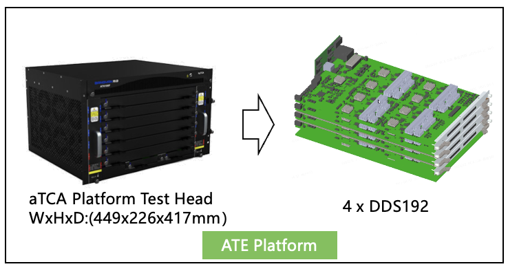
Axis-Tec aTCA ATE platform test head and example four-board DDS192 configuration
Axis-Tec ATEOwn modular electrical test platform

Electrical test foundation

Axis-Tec aTCA ATE platform.

Our modular ATE test head provides the core electrical functions needed by custom test systems and can be combined with the required device interface and automation.

IVIV measurement
I²CDevice communication
I/ODigital control
PSDevice power supply

Test-head size: 449 × 226 × 417 mm · Example shown with 4 × DDS192

ME

Precision mechanics

Motion architecture, probing, fixtures, thermal control and automated material handling.

OP

Optics & instrumentation

Flexible integration with different brands of optical instruments, laser sources, detectors, fibre positioning and free-space optical paths.

SW

Software & data

Integrate customer Python scripts, LabVIEW sequences or C++ modules with recipes, instrument control, mapping and traceability.

Start the conversation

Bring us your next test challenge.

Tell us about your device, measurements, throughput and factory interface. We’ll help shape the platform.

sales@axis-tec.com.sg